India Semiconductor Mission Expansion and Electronics Manufacturing
Source:The Hindu ↗
Why It Matters
Directly relates to India's strategic push for self-reliance in the critical semiconductor supply chain, industrial diversification, and technological capacity building as envisioned under the India Semiconductor Mission. This aligns with GS-III topics on industrial policy and indigenization of technology.
Summary
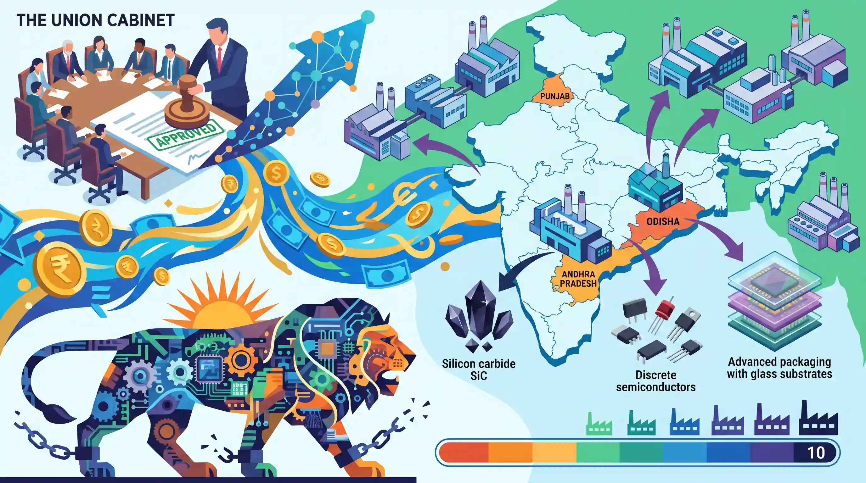
The Union Cabinet has approved four new semiconductor manufacturing and packaging projects worth ₹4,594 crore under the ₹76,000-crore India Semiconductor Mission (ISM). Located in Odisha, Punjab, and Andhra Pradesh, these facilities bring the total number of approved ISM projects to ten. The new plants will focus on specialized, evolving tech segments such as silicon carbide integrated facilities, discrete semiconductors, and advanced packaging with embedded glass substrates. This approval underscores India's strategic push towards self-reliance (Aatmanirbhar Bharat) in critical electronics supply chains and the geographical diversification of its high-tech manufacturing base.
Key Points
- The Union Cabinet approved four new semiconductor projects under the India Semiconductor Mission (ISM), with a total investment of ₹4,594 crore.
- These new facilities will be established in Odisha (Bhubaneswar), Punjab (Mohali), and Andhra Pradesh, expanding the footprint of India's electronics manufacturing ecosystem.
- The projects bring the total number of approved units under the ₹76,000-crore ISM initiative to ten.
- The approved plants focus on specialized and evolving technologies, including silicon carbide manufacturing, discrete semiconductors, and vertically integrated advanced packaging with embedded glass substrates.
- Union Minister Ashwini Vaishnaw highlighted the strategic importance of developing domestic capabilities in silicon carbide technology, an area where institutions like IIT Bhubaneswar are already conducting promising research.
Important Terms
India Semiconductor Mission (ISM)

A ₹76,000-crore initiative launched in 2021 to build a sustainable semiconductor and display ecosystem, providing fiscal support to fabs, chip design, and compound semiconductor units to ensure technological sovereignty.
UPSC context
GS Paper 3: Industrial Policy, S&T; crucial for indigenization, electronic manufacturing, and global supply chain resilience.
SiCSem
A semiconductor manufacturing firm approved to establish India’s first commercial Silicon Carbide (SiC) compound fab in Odisha, focusing on high-voltage components for EVs, defense, and renewable energy.
UPSC context
GS Paper 3: Science and Technology; tests knowledge of niche technologies like compound semiconductors and their industrial applications.
Advanced System in Package (ASIP) Technologies
An Indian company approved to set up an advanced packaging facility in Andhra Pradesh, collaborating with South Korea’s APACT to produce chips for mobile and automotive electronics.
UPSC context
GS Paper 3: Industrial Growth; signifies the shift towards specialized high-tech assembly and testing (OSAT) units in India.
3D Glass Solutions Inc.
A US-based firm approved to build a vertically integrated advanced packaging unit in Odisha, utilizing embedded glass substrate technology for AI, high-performance computing, and defense.
UPSC context
GS Paper 3: S&T; illustrates foreign direct investment (FDI) and technology transfer in cutting-edge electronic manufacturing.
Continental Device India Private Limited (CDIL)
A legacy Indian semiconductor manufacturer expanding its Mohali facility to produce discrete devices (MOSFETs, IGBTs) for the EV and telecom sectors under the ISM framework.
UPSC context
GS Paper 3: Economy; relates to the expansion of brownfield projects and domestic manufacturing capacity.
IIT Bhubaneswar
A premier technical institute hosting the 'NaMo Semiconductor Laboratory' and the 'Silicon-Carbide Research and Innovation Centre,' acting as an R&D and skill-development hub for the semiconductor ecosystem.
UPSC context
GS Paper 2 & 3: Education/S&T; highlights industry-academia collaboration for high-tech skill development and R&D.
Prelims Trap
Discrete semiconductors are advanced integrated circuits containing millions of transistors.
Discrete semiconductors are actually single-function devices (like one diode or transistor). They are strictly distinguished from Integrated Circuits (ICs), which consolidate multiple components.
Static Concepts Connected
What are the core components of the India Semiconductor Mission (ISM)?
- Nodal Agency: Driven by the India Semiconductor Mission under MeitY, operating as an independent business division within the Digital India Corporation.
- Financial Support: Provides up to 50% of the project cost on a pari-passu basis for establishing semiconductor fabs, display fabs, and ATMP/OSAT facilities.
- Ecosystem Focus: Designed to build a complete domestic ecosystem spanning chip design (via the DLI scheme), manufacturing, and advanced packaging.
Why is Silicon Carbide (SiC) considered a next-generation semiconductor?
- Wide Bandgap: SiC has a wide bandgap, allowing the material to operate at much higher voltages and frequencies compared to standard silicon.
- Thermal Efficiency: Its superior heat dissipation minimizes the need for bulky cooling systems, making it highly ideal for aerospace and heavy-duty electric vehicles.
- Power Electronics: It dramatically reduces energy loss during power conversion, significantly boosting battery efficiency in green technologies and smart grids.
Cross-Topic Patterns
SiC chips & the EV Transition
The push for Silicon Carbide (SiC) fabrication directly supports India's e-mobility targets, linking the India Semiconductor Mission (ISM) to the FAME/PM E-DRIVE schemes for electric vehicles.
Geopolitics of Supply Chains
Geographical diversification of domestic semiconductor plants mirrors global 'China-Plus-One' strategies and perfectly aligns with the Quad's Semiconductor Supply Chain Initiative.

Expect a 2026 Prelims S&T question distinguishing between wide-bandgap semiconductors (SiC/GaN) and traditional silicon applications.
Linked PYQs · 1
Linked PYQs · 1
- 2025MainsGS3
India aims to become a semiconductor manufacturing hub. What are the challenges faced by the semiconductor industry in India? Mention the salient features of the India Semiconductor Mission.
