Academia Industry Partnerships in Gallium Nitride Technology
Source:The Hindu ↗
Why It Matters
This partnership highlights the crucial academia-industry collaboration needed to advance specialized semiconductor technologies like Gallium Nitride (GaN) within India, supporting the goals of the India Semiconductor Mission and self-reliance in high-end electronics.
Summary
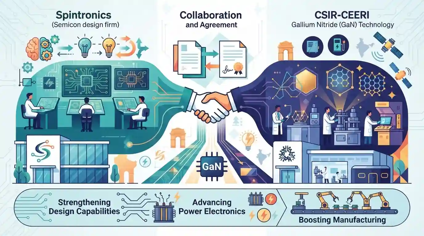
Semicon design firm Spintronics and CSIR-CEERI have inked an agreement to collaborate on Gallium Nitride (GaN) technology, aiming to strengthen India's indigenous capabilities in semiconductor design, power electronics, and advanced electronics manufacturing.
Key Points
- Semicon design firm Spintronics and CSIR-CEERI have signed an agreement for Gallium Nitride (GaN) technology development.
- GaN technology is critical for advanced power electronics, RF applications, and next-gen semiconductor devices due to its high efficiency and thermal conductivity.
- The collaboration bridges industry and research institutions to boost indigenous design and fabrication capabilities in India.
- Aligns with the broader objective of making India a global semiconductor and electronics hub.
Important Terms
India Semiconductor Mission

A specialized wing under the Ministry of Electronics and Information Technology (MeitY) launched in 2021 to spearhead India's semiconductor and display ecosystem development through massive financial incentives.
UPSC context
UPSC Mains GS Paper III (Science & Technology): Indigenization of technology and emerging tech manufacturing policies.
CSIR-CEERI
CSIR-Central Electronics Engineering Research Institute, a premier R&D organization specializing in electronic components, semiconductor devices, and advanced electronics research in India.
UPSC context
UPSC Mains GS Paper III (Science & Technology): Institutional contributions to indigenous research, tech transfer, and R&D.
Spintronics
An emerging semiconductor design firm partnering with domestic research bodies to advance production-ready Gallium Nitride (GaN) power electronics and indigenous manufacturing.
UPSC context
UPSC Mains GS Paper III: Public-private partnerships and startup roles in India's semiconductor mission.
Prelims Trap
Gallium Nitride (GaN) technology is primarily utilized for manufacturing next-generation central processing units and high-density memory chips.
Aspirants might assume Gallium Nitride (GaN) is exclusively used in digital microprocessors, whereas its primary domain is power electronics, RF devices, and high-frequency, high-voltage switching.
Static Concepts Connected
What are Wide Bandgap (WBG) semiconductors and how do they differ from Silicon?
- Bandgap Width: WBG materials like GaN and Silicon Carbide possess a much wider energy bandgap (~3.4 eV for GaN vs 1.1 eV for Silicon).
- Operational Limits: WBG devices can operate at significantly higher voltages, frequencies, and temperatures without thermal breakdown, reducing energy losses.
- Key Applications: Vital for high-power applications including EV fast chargers, 5G RF components, and renewable energy inverters.
Cross-Topic Patterns
GaN Tech & Electric Vehicle Infrastructure
GaN's wide bandgap properties make it indispensable for EV power trains, bridging semiconductor indigenization with green mobility goals under the National Electric Mobility Mission.
CSIR Labs & India Semiconductor Mission
Collaborations between CSIR labs and fabless startups form the bedrock of the India Semiconductor Mission, linking R&D funding with commercial fabrication.

Expect statements testing wide bandgap semiconductors (GaN/SiC) vs traditional silicon in terms of bandgap width, switching speed, and EV/RF utility.
Linked PYQs · 1
Linked PYQs · 1
- 2025MainsGS3
India aims to become a semiconductor manufacturing hub. What are the challenges faced by the semiconductor industry in India? Mention the salient features of the India Semiconductor Mission.
