Semicon 2.0 Focuses on Chip Design Incentives and Domestic Innovation
Source:Indian Express ↗
Why It Matters
Semiconductors are critical for modern electronics, defense, and economic security. Understanding India's transition from manufacturing subsidies to design-focused incentives under Semicon 2.0 is vital for GS3 (Economy & Science and Technology) questions on industrial policy and high-tech manufacturing.
Summary
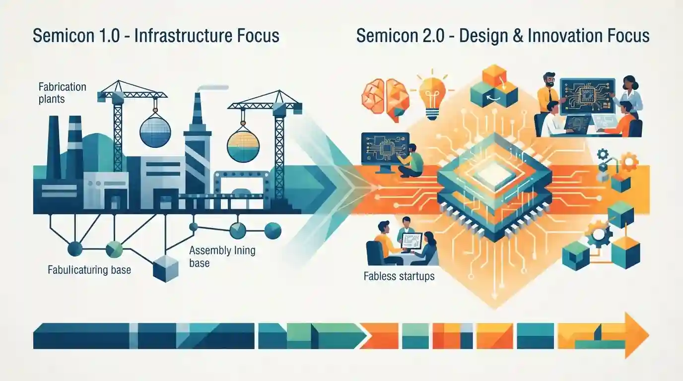
The article discusses India's strategic push towards semiconductor design incentives under the expanded 'Semicon 2.0' policy framework. While the initial phase focused on building fabrication and assembly infrastructure, the new phase emphasizes strengthening chip design capabilities, supporting fabless startups, and fostering indigenous intellectual property to make India a holistic semiconductor hub.
Key Points
- India is pushing for the next phase of its semiconductor mission (Semicon 2.0), focusing heavily on semiconductor design, research, and intellectual property creation.
- The initial push primarily targeted fabrication units (fabs) and display units through capital subsidies, while Semicon 2.0 expands incentives to fabless chip design startups and local design ecosystems.
- Design incentives aim to reduce India's reliance on foreign chip design houses, foster domestic product innovation, and strengthen the electronics value chain.
- Challenges include a shortage of specialized talent, high initial R&D costs, and global supply chain dependencies.
Important Terms
Semicon India Programme

A comprehensive central government scheme providing financial support and infrastructure incentives to build a vibrant semiconductor, display manufacturing, and design ecosystem in India.
UPSC context
Important for GS Paper III (Technology, Industrial Policy, Manufacturing Growth); tests understanding of India's flagship high-tech industrial policy.
Design Linked Incentive (DLI) Scheme
A core component of the Semicon India Programme offering financial incentives and design infrastructure support to startups, MSMEs, and domestic companies for designing semiconductor chips and IP.
UPSC context
Important for GS Paper III (Technology Missions, IT & Computers); tests knowledge of specific policy tools promoting indigenous chip design.
India Semiconductor Mission
An institutional mechanism under MeitY tasked with driving India's semiconductor and display ecosystem vision, acting as the nodal agency for executing semiconductor policies.
UPSC context
Important for GS Paper III (Science & Technology - Institutional Frameworks); tests governance structures for critical technology missions.
Ministry of Electronics and Information Technology
The nodal union ministry responsible for formulating policies related to information technology, electronics, and internet diffusion, which oversees India's semiconductor and digital manufacturing missions.
UPSC context
Important for GS Paper II and III (Governance and Technology); tests knowledge of key administrative bodies handling digital and hardware policies.
Prelims Trap
India's semiconductor incentives are exclusively restricted to capital subsidies for setting up fabrication (fab) and display units.
Aspirants often assume India's semiconductor mission is solely about setting up fabrication plants (fabs), ignoring that Semicon 2.0 specifically expands incentives to upstream materials, equipment, and downstream fabless design.
Static Concepts Connected
What are the primary institutional mechanisms and incentive structures under India's Semiconductor Mission?
- ISM Mandate: Nodal Body: Functioning under the Ministry of Electronics and Information Technology (MeitY) as a dedicated independent business division.
- Capex Subsidies: Fiscal Support: Capital support up to 50% of project cost for semiconductor fabs, display fabs, and compound semiconductor facilities.
- DLI Scheme: Design Support: The Design Linked Incentive (DLI) scheme offers financial incentives and deployment-linked support for domestic chip design startups.
Cross-Topic Patterns
Semiconductors & Manufacturing Industrial Policy Linkages
India's push into semiconductor manufacturing under ISM mirrors the capital-intensive production-linked incentive (PLI) frameworks deployed across 14 sunrise sectors to enhance manufacturing share in GDP.
Phased Localization & Value Chain Upgradation
The transition from assembly-only to indigenous design in semiconductors mirrors the phased manufacturing program (PMP) used previously in mobile phone components.

Expect statement-based questions distinguishing India's initial fab-centric push from Semicon 2.0's expanded focus on design and materials.
Linked PYQs · 2
Linked PYQs · 2
- 2025MainsGS3
India aims to become a semiconductor manufacturing hub. What are the challenges faced by the semiconductor industry in India? Mention the salient features of the India Semiconductor Mission.
- 2025MainsGS3
Discuss the rationale of the Production Linked Incentive (PLI) scheme. What are its achievements? In what way can the functioning and outcomes of the scheme be improved?
