Semicon 2.0 Focuses on Chip and Semiconductor Design Incentives
Source:Indian Express ↗
কেন এটি গুরুত্বপূর্ণ
Semiconductors are foundational to modern technology, strategic security, and economic growth. Understanding the shift from mere assembly to design-led incentives (Semicon 2.0) is vital for GS3 (Technology/Indigenization).
সারসংক্ষেপ
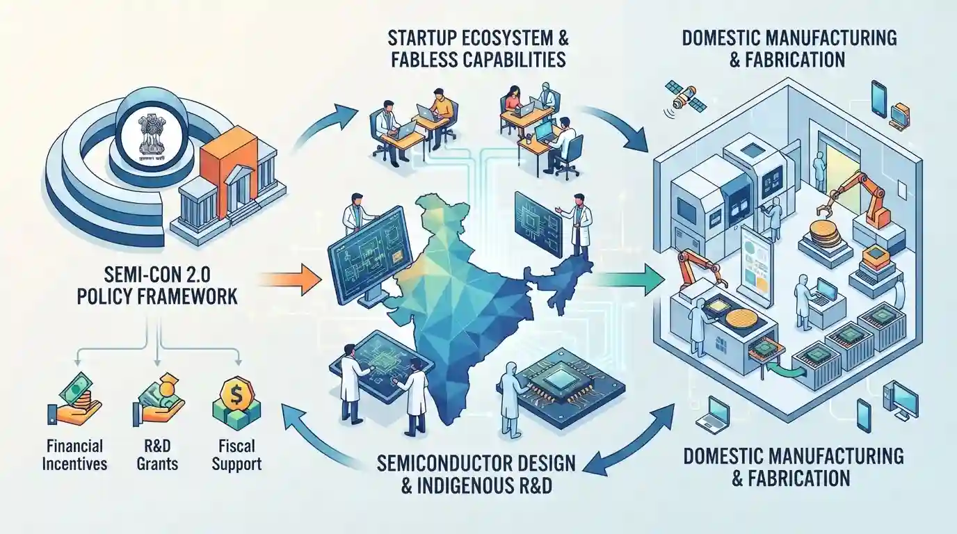
The article highlights the policy push under 'Semincon 2.0' to expand India's semiconductor strategy by prioritizing chip and semiconductor design incentives alongside manufacturing, strengthening indigenous R&D and fabless capabilities.
মূল বিষয়
- Semincon 2.0 focuses heavily on boosting chip and semiconductor design incentives in India.
- Moving beyond pure manufacturing and assembly (OSAT), the push emphasizes domestic intellectual property, design start-ups, and fabless ecosystem development.
- Crucial for achieving technological self-reliance, reducing import dependency, and fostering high-value R&D jobs in critical electronic infrastructure.
গুরুত্বপূর্ণ শব্দ
Semicon 2.0

An ambitious central government policy scheme notified with a multi-lakh crore outlay to consolidate India's semiconductor value chain by incentivizing chip design, wafer fabs, packaging, equipment, materials, R&D, and talent creation.
UPSC context
Relevant for GS Paper III (Technology, Government Policies). Tests understanding of India's strategic push for high-tech manufacturing, self-reliance, and electronics indigenization.
India Semiconductor Mission (ISM)
The nodal government agency established under MeitY to drive India's long-term strategies for semiconductor and display manufacturing ecosystems, vetting investments and executing incentive programs.
UPSC context
Important for GS Paper III (Indigenization of Technology). Evaluates institutional frameworks designed to implement critical industrial policies and secure tech supply chains.
Ministry of Electronics and Information Technology (MeitY)
The Union ministry responsible for formulating policies related to information technology, electronics, and internet diffusion, anchoring national initiatives like the semiconductor mission and digital infrastructure.
UPSC context
Important for GS Paper II and III (Governance and Technology). Tests knowledge of key ministries spearheading digital governance and high-tech manufacturing policies.
সংযুক্ত স্থির ধারণা
What is the difference between a semiconductor foundry, an OSAT facility, and a fabless design house?
- Foundry role: Silicon wafers are fabricated into integrated circuits using specialized chemicals and photolithography.
- OSAT facility: Tested, packaged, and assembled after fabrication before entering electronic assemblies.
- Fabless firm: Specializes exclusively in research, architecture, and chip design without owning physical manufacturing units.
আন্তঃবিষয় প্যাটার্ন
Semiconductors + Defense Indigenization Linkages
Semicon 2.0 links the Make in India initiative with advanced technology indigenization, mirroring past thrusts in defense indigenization via iDEX and the Technology Development Fund.

Expect a multi-statement Prelims question comparing Design-Linked Incentives (DLI) with capital subsidy schemes for OSAT and fabrication units.
সংযুক্ত PYQ · 3
সংযুক্ত PYQ · 3
- 2025MainsGS3
India aims to become a semiconductor manufacturing hub. What are the challenges faced by the semiconductor industry in India? Mention the salient features of the India Semiconductor Mission.
- 2026PrelimsGS1
Which one of the following pairs of semiconductor plants in India and their locations is not correctly matched ?
- 2026PrelimsGS1
Which of the following statements about DHRUV64 is/are correct? 1. It is the third chip fabricated under the DIR-V Programme with an overall aim to enable the creation of microprocessors for India. 2. It is India's first homegrown 1.0 GHz, 64-bit dual-core microprocessor. Select the answer using the code given below :
