Qualcomm Designs 2nm Chip in India to Boost Semiconductor Ecosystem
Source:Indian Express ↗
Why It Matters
This highlights India's strategic shift up the technology value chain in the highly critical semiconductor industry. It is highly relevant for GS3 questions on the India Semiconductor Mission, self-reliance in electronics, and harnessing demographic dividend in deep-tech sectors.
Summary
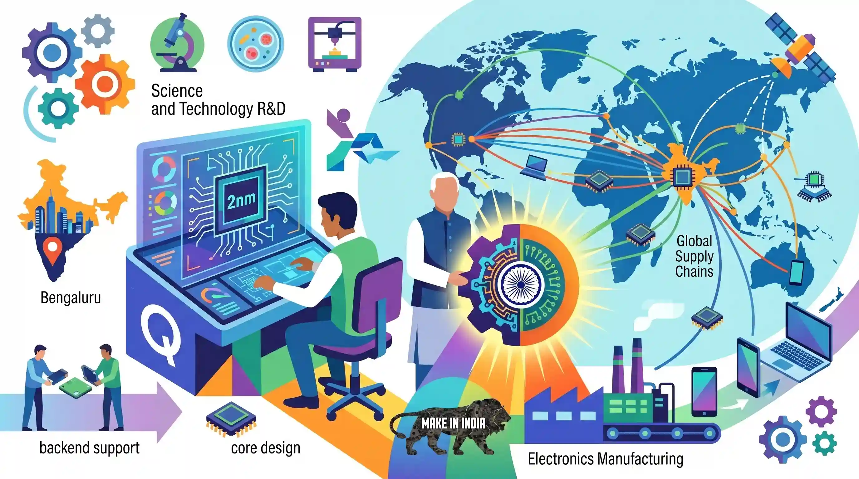
Qualcomm has successfully designed a cutting-edge 2nm semiconductor chip entirely at its Bengaluru facility, marking a significant milestone for India's technology sector. With its largest engineering workforce outside the US located in India, Qualcomm's achievement reflects India's evolution into a core hub for complex global semiconductor design rather than just backend support. Union Minister Ashwini Vaishnaw hailed this development as a boost to India's semiconductor design ecosystem, aligning with the country's broader ambitions under the India Semiconductor Mission to establish a strong presence in the global electronics supply chain.
Key Points
- Qualcomm has achieved a breakthrough by completing the design of a 2nm semiconductor chip entirely at its Bengaluru facility.
- India hosts Qualcomm's largest engineering workforce outside the United States, underscoring the country's growing importance in global tech innovation.
- The development highlights India's transition from backend support roles to leading complex, high-end semiconductor design and R&D.
- Union Minister Ashwini Vaishnaw noted this achievement as a major milestone for India's semiconductor design ecosystem and the 'Make in India' initiative.
Important Terms
India Semiconductor Mission (ISM)

A nodal agency under the Ministry of Electronics and IT, launched with ₹76,000 crore to establish a sustainable semiconductor and display ecosystem through financial incentives and strategic partnerships.
UPSC context
GS Paper 3 (Industrial Policy/Economy); critical for questions on technological self-reliance, manufacturing hubs, and global electronics value chains.
2nm (2-Nanometer) Technology
A cutting-edge semiconductor manufacturing process node where transistor miniaturization allows for significantly higher density, leading to nearly 45% faster processing and 30% lower power consumption than previous generations.
UPSC context
GS Paper 3 (Science & Tech); relevant to emerging technologies, AI hardware, and India's transition from service-based to high-end product R&D.
Tape-out
The final stage of the semiconductor design process where the electronic circuit layout is completed and sent to the fabrication facility (foundry) for physical manufacturing.
UPSC context
GS Paper 3 (S&T); specific technical term marking a milestone in indigenous design capabilities and product development.
Fabless Manufacturing
A business model where a company (like Qualcomm) focuses on designing and marketing chips while outsourcing the capital-intensive physical fabrication to specialized foundries like TSMC or Samsung.
UPSC context
GS Paper 3 (Economy/IT); represents India's core strength in the global semiconductor hierarchy, utilizing its 20% share of global design talent.
Design Linked Incentive (DLI) Scheme
A sub-scheme under ISM that provides financial and infrastructural support to domestic startups and MSMEs involved in semiconductor design for Integrated Circuits and System-on-Chips.
UPSC context
GS Paper 3 (Government Schemes); essential for understanding how India incentivizes local innovation and IP creation in high-tech sectors.
Semiconductor Ecosystem
The interconnected network of design houses, fabrication units (fabs), assembly, testing, marking, and packaging (ATMP) facilities, and supporting industries like chemicals and ultrapure water production.
UPSC context
GS Paper 3 (Infrastructure); tests the holistic understanding of supply chain resilience and the multi-tiered requirements of high-tech manufacturing.
Prelims Trap
"India has recently achieved domestic manufacturing and fabrication capabilities for cutting-edge 2nm semiconductor chips."
The 2nm breakthrough in Bengaluru is strictly for chip design (fabless ecosystem). India does not yet physically manufacture or fabricate advanced 2nm chips.
Static Concepts Connected
What does a smaller nanometer (nm) node signify in semiconductor technology?
- Transistor Density: Smaller nodes allow more transistors to be packed into the same physical area on the chip.
- Processing Performance: Higher density enables significantly faster processing speeds, critical for advanced computing and AI.
- Power Efficiency: Smaller nodes reduce the distance electrons must travel, resulting in less power consumption and heat generation.
How does the Design Linked Incentive (DLI) differ from general fabrication support?
- Target Phase: DLI reimburses up to 50% of eligible expenditure for the conceptualization and design phase of ICs and chipsets.
- Fabless Focus: It supports India's "fabless" ecosystem—companies that design chips but outsource the physical manufacturing to foundries elsewhere.
- Sales Incentives: DLI provides a deployment-linked incentive of 4% to 6% on net sales of the successfully designed semiconductor products.
Cross-Topic Patterns
Fabless design meets global geopolitics
India's rising dominance in IC design complements strategic tech-alliances like the US-led Chip 4 Alliance, which aim to de-risk semiconductor supply chains from China.
Critical minerals + Semiconductor fabs
Transitioning India's success from software/design to physical semiconductor fabrication will heavily depend on securing supply chains for critical minerals like Gallium and Germanium.

Semiconductor design (DLI scheme) vs physical fabrication distinctions will likely form a multi-statement tech question in 2026 Prelims.
Linked PYQs · 1
Linked PYQs · 1
- 2025MainsGS3
India aims to become a semiconductor manufacturing hub. What are the challenges faced by the semiconductor industry in India? Mention the salient features of the India Semiconductor Mission.
