Precision Manufacturing Ecosystem for India Semiconductor Mission
Source:PIB ↗
Why It Matters
Understanding the upstream linkages, precision manufacturing requirements, and localized supply chain ecosystems essential for the success of India's semiconductor mission is critical for GS3 Science & Technology and Economic Development questions.
Summary
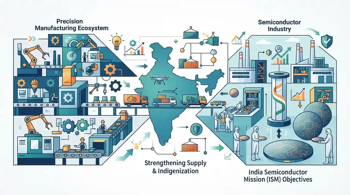
The article discusses how a robust precision manufacturing ecosystem is fast becoming a vital catalyst and structural backbone for India's burgeoning semiconductor sector, strengthening local supply chains, reducing import dependencies, and bolstering the objectives of the India Semiconductor Mission (ISM).
Key Points
- Precision manufacturing and local tool-and-die ecosystems are emerging as core structural enablers for India's upcoming semiconductor fabs and OSAT facilities.
- Scaling the domestic semiconductor industry requires deep integration of high-precision components, chemical supply chains, and specialized engineering talent.
- The growth of a local precision manufacturing ecosystem helps minimize supply chain vulnerabilities and positions India as a resilient global hub under the India Semiconductor Mission (ISM).
Important Terms
India Semiconductor Mission

A specialized nodal agency under the Ministry of Electronics and Information Technology (MeitY) tasked with driving India's semiconductor and display ecosystem strategies.
UPSC context
GS Paper III (Technology / Economic Development): Tests knowledge of government policies for high-tech manufacturing and self-reliance.
Ministry of Electronics and Information Technology (MeitY)
The nodal central ministry responsible for formulating policies related to IT, electronics, and internet proliferation, overseeing strategic programs like the India Semiconductor Mission.
UPSC context
GS Paper II/III (Governance / IT Policy): Tests understanding of institutional frameworks driving digital governance and manufacturing in India.
Prelims Trap
The India Semiconductor Mission is exclusively focused on financing large greenfield silicon fabrication (fab) units.
Aspirants often assume the India Semiconductor Mission only finances large fabrication plants (fabs), ignoring that OSAT, advanced packaging, and precision tool ecosystems are equally central components.
Static Concepts Connected
What are the key operational stages and differences between semiconductor Fabs and OSAT facilities?
- Fabrication (Fab): Silicon Wafers are processed into integrated circuits using photolithography and etching in capital-intensive cleanrooms.
- OSAT Facilities: Outsourced Assembly and Test involves dicing, packaging, and testing manufactured silicon wafers for end-use.
- Ecosystem Entry: OSAT facilities require lower capital outlays than Fabs and form the immediate entry point for domestic semiconductor ecosystems.
Cross-Topic Patterns
Semiconductors + Environmental Clearance Standards
The push for domestic semiconductor fabs requires ultra-pure electronic gases and water, linking high-end manufacturing with strict environmental clearances and chemical safety standards.
Semiconductor Mission + PLI Schemes for Manufacturing
Building domestic fabs and OSAT units directly anchors the Production Linked Incentive (PLI) scheme, testing whether fiscal subsidies can successfully crowd-in private high-tech capital.

Expect a statement-based question pairing Semicon 2.0 fiscal outlays with specific OSAT and precision manufacturing prerequisites.
Linked PYQs · 2
Linked PYQs · 2
- 2025MainsGS3
India aims to become a semiconductor manufacturing hub. What are the challenges faced by the semiconductor industry in India? Mention the salient features of the India Semiconductor Mission.
- 2026PrelimsGS1
Which one of the following pairs of semiconductor plants in India and their locations is not correctly matched ?
