DLI Scheme Success in Indigenous Semiconductor Chip Design
Source:PIB ↗
ఇది ఎందుకు ముఖ్యం
India is actively pushing to become a global semiconductor hub to reduce import dependence and ensure strategic autonomy in electronics. Successes under the DLI Scheme and the development of indigenous microprocessors (like VEGA) are direct examples of 'Aatmanirbhar Bharat' in high-technology sectors, highly relevant for GS3 S&T and Economy.
సారాంశం
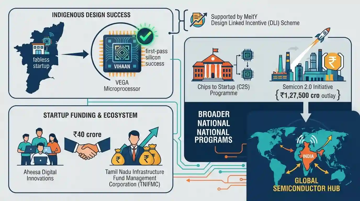
The article highlights a significant milestone for India's semiconductor ecosystem as Chennai-based fabless startup Aheesa Digital Innovations achieved first-pass silicon success with 'VIHAAN', a broadband chip integrating the indigenous VEGA Microprocessor (developed by C-DAC). Supported by the government's Design Linked Incentive (DLI) Scheme under MeitY, this achievement demonstrates India's growing self-reliance in fabless chip design and deep-tech innovation. Aheesa's success in raising ₹40 crore from the Tamil Nadu Infrastructure Fund Management Corporation (TNIFMC) underscores growing investor confidence in the sector. This aligns with broader national efforts, including the Chips to Startup (C2S) Programme and the newly approved Semicon 2.0 initiative with a ₹1,27,500 crore outlay, aiming to position India as a global semiconductor hub.
ముఖ్య అంశాలు
- Chennai-based fabless startup Aheesa Digital Innovations successfully developed 'VIHAAN', a broadband network System on Chip (SoC).
- The VIHAAN chip integrates the 'VEGA Microprocessor', which was indigenously developed by the Centre for Development of Advanced Computing (C-DAC).
- The development was supported by the Ministry of Electronics and IT's (MeitY) Design Linked Incentive (DLI) Scheme, which fosters semiconductor design innovation in India.
- Aheesa raised ₹40 crore from the Tamil Nadu Infrastructure Fund Management Corporation (TNIFMC), demonstrating strong VC confidence in Indian deep-tech startups.
- The Indian government recently approved 'Semicon 2.0' with an outlay of ₹1,27,500 crore to further boost the semiconductor manufacturing and design ecosystem.
ముఖ్యమైన పదాలు
Design Linked Incentive (DLI) Scheme

A central government initiative under the India Semiconductor Mission providing financial incentives and design infrastructure support to domestic startups, MSMEs, and companies involved in fabless semiconductor chip design.
UPSC context
GS Paper 3: S&T (Indigenization) and Economy (Industrial Policy). Tests understanding of semiconductor manufacturing policies.
Chips to Startup (C2S) Programme
A national capacity-building initiative under MeitY designed to train 85,000 industry-ready VLSI and embedded system professionals, support design startups, and facilitate indigenous IP creation and chip fabrication.
UPSC context
GS Paper 3: S&T (Skill Development). Tests knowledge of tech education and capacity-building schemes.
Semicon 2.0
The second phase of the India Semiconductor Mission, approved with a ₹1,27,500 crore outlay, aimed at developing an integrated ecosystem including chip design, machinery, specialty materials, R&D, and talent.
UPSC context
GS Paper 3: Economy (Industrial Policy). Tests strategic understanding of self-reliance and tech-manufacturing infrastructure.
Centre for Development of Advanced Computing (C-DAC)
A premier R&D institution under MeitY that designs high-performance computing systems and serves as the nodal implementing agency for key national initiatives like DLI and C2S.
UPSC context
GS Paper 3: S&T (Institutional framework). Tests awareness of public institutions driving domestic tech development.
VEGA Microprocessor
A portfolio of indigenously developed, 32-bit and 64-bit multi-core processors based on the open-source RISC-V architecture, created by C-DAC to secure domestic self-reliance in chip design.
UPSC context
GS Paper 3: S&T (Indigenization of Technology). Tests awareness of domestic technological breakthroughs.
Ministry of Electronics and Information Technology (MeitY)
The executive ministry responsible for formulating policies on electronics, information technology, and cyber security, as well as overseeing the India Semiconductor Mission.
UPSC context
GS Paper 2: Governance. Tests knowledge of executive structures steering digital governance and tech manufacturing.
ప్రిలిమ్స్ ఉచ్చు
MeitY's Design Linked Incentive (DLI) scheme primarily offers fiscal incentives based on the volume of physical silicon wafers fabricated.
DLI targets pre-fabrication 'fabless' design stages (IP creation, prototyping, EDA access). Physical fabrication and manufacturing volumes are incentivized under separate PLI / Semicon schemes.
అనుసంధానమైన స్థిర భావనలు
What is RISC-V Architecture and its national significance?
- Open-source design: It is a royalty-free, open-standard instruction set architecture, allowing developers to design custom processors without foreign licensing fees.
- Strategic autonomy: Allows India to build backdoor-free custom microprocessors (like SHAKTI and VEGA), securing critical military and civilian infrastructure.
How do Fabless and Foundry semiconductor models differ?
- Fabless model: Firms focus exclusively on chip design and IP development, avoiding the massive capital expenditure of building fabrication plants.
- Foundry model: Highly capital-intensive commercial plants that physically manufacture silicon wafers based on designs provided by fabless clients.
అంతర-అంశ నమూనాలు
Semiconductors and strategic autonomy
Leveraging open-source RISC-V protects India from foreign tech sanctions and global supply chain disruptions, reinforcing cyber-security in critical infrastructure and defense systems.
Deep-tech funding and economic federalism
Co-investment by MeitY's central DLI scheme and state-backed funds like TNIFMC shows a growing trend of collaborative federalism to finance high-gestation deep-tech ventures.

Expect questions mapping RISC-V processors (SHAKTI/VEGA) to developers, alongside structural parameters of MeitY's DLI scheme.
అనుసంధాన PYQలు · 4
అనుసంధాన PYQలు · 4
- 2025MainsGS3
India aims to become a semiconductor manufacturing hub. What are the challenges faced by the semiconductor industry in India? Mention the salient features of the India Semiconductor Mission.
- 2025MainsGS3
Discuss the rationale of the Production Linked Incentive (PLI) scheme. What are its achievements? In what way can the functioning and outcomes of the scheme be improved?
- 2026PrelimsGS1
Which of the following statements about DHRUV64 is/are correct? 1. It is the third chip fabricated under the DIR-V Programme with an overall aim to enable the creation of microprocessors for India. 2. It is India's first homegrown 1.0 GHz, 64-bit dual-core microprocessor. Select the answer using the code given below :
- 2026PrelimsGS1
Which one of the following pairs of semiconductor plants in India and their locations is not correctly matched ?
