NIELIT and SCL Mohali launch indigenous process design kit
Source:PIB ↗
આ શા માટે મહત્વનું છે
Highlights key infrastructural and capacity-building measures (eChipHub and PDK availability) undertaken by the government to support the India Semiconductor Mission. It provides a concrete example for answers on India's efforts to become a global semiconductor hub and reduce import dependence.
સારાંશ
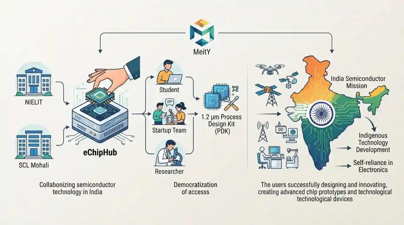
The National Institute of Electronics and Information Technology (NIELIT) and Semiconductor Laboratory (SCL) Mohali have collaborated to make India's indigenous 1.2 µm Process Design Kit (PDK) available on the eChipHub platform. Funded by MeitY, the eChipHub initiative seeks to democratize chip design for students, startups, and researchers across the country. This partnership directly supports the India Semiconductor Mission (ISM) by enhancing capacity building, promoting indigenous technology development, and advancing self-reliance in electronics and semiconductor manufacturing under the Atmanirbhar Bharat vision.
મુખ્ય મુદ્દા
- NIELIT and SCL Mohali have partnered to make the indigenous 1.2 µm Process Design Kit (PDK) available on the eChipHub platform.
- eChipHub is managed by NIELIT under a MeitY-funded project to democratize chip design and development for students, researchers, and startups.
- The initiative bolsters the India Semiconductor Mission (ISM) by fostering an indigenous semiconductor ecosystem and promoting self-reliance in high-tech manufacturing.
- This collaboration emphasizes capacity building and skill development in emerging technologies to support India's electronics manufacturing goals.
મહત્વપૂર્ણ શબ્દો
India Semiconductor Mission (ISM)

A specialized independent division under the Digital India Corporation that serves as the nodal agency for building a self-reliant domestic semiconductor and display manufacturing ecosystem in India.
UPSC context
GS Paper III (Science & Tech), testing knowledge of industrial policies, digital infrastructure, and chip manufacturing ecosystems.
Atmanirbhar Bharat
A nationwide campaign launched in 2020 by the Government of India aimed at achieving economic self-reliance, boosting local manufacturing, reducing import dependence, and integrating India into global supply chains.
UPSC context
GS Paper III (Indian Economy), assessing national self-reliance, industrial reforms, and manufacturing growth strategies.
Semiconductor Laboratory (SCL) Mohali
India's only government-owned integrated device manufacturer and semiconductor fabrication unit, operating under MeitY, which designs, fabricates, and tests chips for strategic sectors like space and defense.
UPSC context
GS Paper III (Indigenization of Technology), examining public sector contributions to strategic electronics and domestic fabrication capabilities.
National Institute of Electronics and Information Technology (NIELIT)
An autonomous scientific society under MeitY, responsible for human resource development, capacity building, and providing formal and non-formal training in information technology, electronics, and digital skills.
UPSC context
GS Paper II (Governance/Education), evaluating public sector capacity-building, skill development initiatives, and digital literacy.
Ministry of Electronics and Information Technology (MeitY)
A union ministry of India responsible for formulating and implementing policies related to information technology, electronics manufacturing, e-governance, digital public infrastructure, and cyber security.
UPSC context
GS Paper II & III (Governance/Science), testing institutional frameworks for digital governance and electronics policies.
પ્રિલિમ્સ ટ્રેપ
The Semiconductor Laboratory (SCL) Mohali operates under the administrative control of the Department of Space (ISRO).
SCL Mohali was transferred from the Department of Space (ISRO) to MeitY in February 2022 to align it with national commercial semiconductor goals.
સંલગ્ન સ્થિર ખ્યાલો
What is a Process Design Kit (PDK) in semiconductor manufacturing?
- Digital blueprint: It is a set of files, layout rules, and transistor simulation models specific to a foundry’s technology node.
- Bridge function: It acts as the essential interface allowing fabless design startups to build chips compatible with physical manufacturing plants.
- Yield assurance: Ensures that a designer's software layout will physically function and achieve economic yield when manufactured.
What is the India Semiconductor Mission (ISM)?
- Nodal agency: A specialized division under the Digital India Corporation built to drive India's semiconductor and display ecosystem.
- Financial support: Administers financial support schemes (up to 50% project cost) for setting up Silicon Fabs, Display Fabs, and OSAT facilities.
- Design-led focus: Nurtures domestic design companies through financial and infrastructural support like the Design Linked Incentive (DLI) scheme.
આંતર-વિષય પેટર્ન
Dual-use tech: Space to commercial pivot
SCL Mohali’s transition from space-grade chips to open-access PDKs showcases India's policy shift toward commercializing strategic state-owned technology assets.
Digital Public Infrastructure for R&D
Integrating Aadhaar authentication with open-source EDA tools on eChipHub mirrors India's DPI model, democratizing expensive chip design tools for startups.

SCL Mohali's shift to MeitY and PDK access on eChipHub highlight India's focus on design-level indigenization under Semicon 2.0.
સંલગ્ન PYQ · 1
સંલગ્ન PYQ · 1
- 2025MainsGS3
India aims to become a semiconductor manufacturing hub. What are the challenges faced by the semiconductor industry in India? Mention the salient features of the India Semiconductor Mission.
