Indias First Three D Chip Packaging Facility
Source:Indian Express ↗
Why It Matters
Semiconductors are a pivotal geopolitical asset. For UPSC aspirants, understanding the distinction between chip fabrication and advanced packaging (like 3D packaging) is essential for Science & Technology. Furthermore, analysing the impact of the India Semiconductor Mission and PLI schemes on the manufacturing sector is highly relevant for GS3 Mains.
Summary
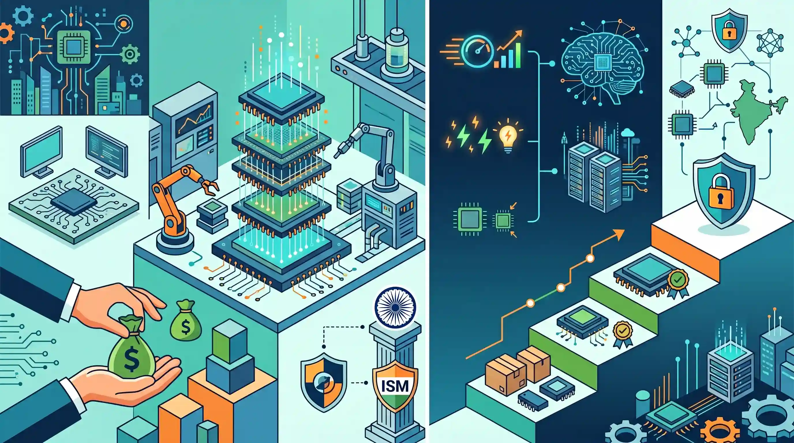
The article details the establishment of India's first 3D chip packaging plant, marking a significant milestone in the country's journey toward semiconductor self-reliance. Unlike traditional 2D packaging, 3D packaging stacks integrated circuits vertically, yielding higher performance, reduced power consumption, and smaller form factors—attributes essential for advanced applications like Artificial Intelligence (AI) and high-performance computing. Driven by the India Semiconductor Mission (ISM) and heavily supported by government production-linked incentives, this development helps India move up the global electronics value chain, shifting from basic assembly (OSAT) to advanced Assembly, Testing, Marking, and Packaging (ATMP) technologies while securing strategic supply chains.
Key Points
- Concept of 3D Chip Packaging: Involves vertically stacking semiconductor chips (Integrated Circuits) to function as a single device, which drastically reduces signal travel distance, increases processing speed, lowers power consumption, and saves physical space.
- Shift to Advanced Packaging: The establishment of India's first 3D chip packaging plant marks a crucial leap from basic OSAT (Outsourced Semiconductor Assembly and Test) to advanced ATMP (Assembly, Testing, Marking, and Packaging) capabilities.
- Role of the India Semiconductor Mission (ISM): Under the ISM, the government provides up to 50% capital expenditure support (augmented by state subsidies) to attract domestic and global players to set up advanced electronics manufacturing facilities.
- Strategic and Geopolitical Value: Developing domestic packaging and fabrication capabilities reduces import dependence, shields India from global supply-chain bottlenecks, and secures critical hardware for strategic sectors like defence, AI, and telecommunications.
Important Terms
India Semiconductor Mission (ISM)

A specialized business division under the Digital India Corporation implementing a ₹76,000-crore program to develop India's semiconductor and display manufacturing ecosystem through fiscal support and strategic collaborations.
UPSC context
GS-III (Economy/S&T); evaluates knowledge of industrial policy, strategic self-reliance, and electronics manufacturing hubs.
3D Chip Packaging
An advanced technology where multiple integrated circuits are stacked vertically rather than horizontally, enhancing performance, reducing power consumption, and enabling higher density for AI and high-performance computing.
UPSC context
GS-III (S&T); tests understanding of emerging technologies and India's entry into high-value semiconductor value chain segments.
ATMP (Assembly, Testing, Marking, and Packaging)
The backend stage of semiconductor manufacturing where fabricated silicon wafers are cut, assembled into protective cases, tested for quality, and marked for final distribution.
UPSC context
GS-III (S&T/Economy); relevant for questions on the semiconductor manufacturing lifecycle and domestic value addition.
Production Linked Incentive (PLI) Scheme
A performance-driven initiative offering financial incentives (typically 4-6%) to manufacturers based on incremental sales of domestically produced goods in 14 strategic sectors, including electronics.
UPSC context
GS-III (Economy); central to topics on "Make in India," export competitiveness, and boosting manufacturing GDP.
Design Linked Incentive (DLI) Scheme
A fiscal program providing financial and infrastructure support to domestic startups and MSMEs for semiconductor design, development, and deployment of indigenous Intellectual Property (IP).
UPSC context
GS-III (Economy/S&T); highlights the shift toward design-led self-reliance and "fabless" chip innovation.
Prelims Trap
"India's first 3D chip plant manufactures the raw silicon semiconductor wafers."
ATMP/OSAT plants package and assemble existing chips into usable components; they do not fabricate the raw silicon wafers themselves (which is done by Fabs).
Static Concepts Connected
What is the difference between Fabs, OSAT, and ATMP?
- Fabrication (Fabs): The highly capital-intensive front-end process where microscopic integrated circuits are printed onto bare silicon wafers.
- OSAT: Outsourced Semiconductor Assembly and Test; third-party vendors handling the basic backend assembly and testing of fabricated chips.
- ATMP: Assembly, Testing, Marking, and Packaging; a broader term for backend operations, now evolving to include complex 3D integration of multiple chips.
How does 3D Heterogeneous Integration (3DHI) bypass Moore's Law?
- Moore's Law Limits: As transistors shrink to near-atomic sizes, placing more on a single 2D chip leads to severe overheating and quantum tunneling issues.
- Vertical Stacking: 3DHI vertically stacks different types of chips (logic, memory, sensors) made from varying materials into a single interconnected package.
- Glass Substrates: Advanced 3D packaging uses specialized glass instead of silicon/organic substrates, offering superior thermal management and lower electrical signal loss.
Cross-Topic Patterns
Semiconductor ATMP + Quad Tech Initiatives
Domestic ATMP plants build hardware security for critical sectors, directly aligning with the Quad's objective to secure semiconductor supply chains away from Chinese dominance.
ISM + Regional Industrial Diversification
The establishment of advanced plants in Odisha and Assam highlights how the India Semiconductor Mission is decentralizing high-tech manufacturing beyond traditional southern hubs.

Expect a multi-statement question on 3D heterogeneous integration and glass substrates bypassing Moore's Law limits in 2026.
Linked PYQs · 3
Linked PYQs · 3
- 2025MainsGS3
India aims to become a semiconductor manufacturing hub. What are the challenges faced by the semiconductor industry in India? Mention the salient features of the India Semiconductor Mission.
- 2025MainsGS3
Discuss the rationale of the Production Linked Incentive (PLI) scheme. What are its achievements? In what way can the functioning and outcomes of the scheme be improved?
- 2018PrelimsGS1
"3D printing" has applications in which of the following? 1. Preparation of confectionery items 2. Manufacture of bionic ears 3. Automotive industry 4. Reconstructive surgeries 5. Data processing technologies Select the correct answer using the code given below:
