IBM Unveils World First Sub-1 Nanometre Chip Technology
Source:Indian Express ↗
Why It Matters
Understanding cutting-edge semiconductor nodes (like sub-1 nm) is vital as India strategically invests in the India Semiconductor Mission. This technology determines global supremacy in emerging fields such as generative AI, cloud infrastructure, and national security computing capabilities.
Summary
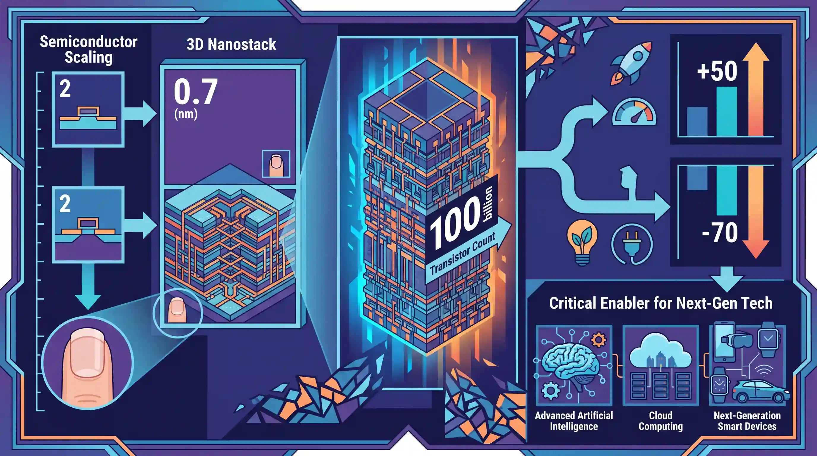
IBM has announced a groundbreaking sub-1 nanometre (0.7 nm) semiconductor chip, utilizing a novel 3D 'nanostack' architecture to pack 100 billion transistors into a fingernail-sized area. This leap beyond the traditional nanometre era promises a 50% performance boost or a 70% reduction in energy usage over current 2nm chips, serving as a critical enabler for advanced artificial intelligence, cloud computing, and next-generation smart devices.
Key Points
- IBM has unveiled the world's first sub-1 nanometre (0.7 nm or 7 angstrom node) chip technology, pushing semiconductor manufacturing to an atomic scale.
- The breakthrough relies on a new 3D 'nanostack' architecture that stacks transistors vertically, allowing around 100 billion transistors on a fingernail-sized chip.
- The new node promises up to 50% higher performance or 70% greater energy efficiency compared to IBM's 2021 2nm chip technology.
- This advancement is positioned to meet the escalating computational and energy demands of generative AI, cloud infrastructure, and future electronics.
Important Terms
sub-1 nanometre chip

Semiconductor technology with transistor nodes measuring less than one nanometre (e.g., 0.7 nm). It marks the industry's transition from nanometre-scale to atomic-scale (angstrom) manufacturing.
UPSC context
GS Paper 3: Science and Technology. Relevant for breakthroughs in nanotechnology and global semiconductor competition.
3D nanostack architecture
A semiconductor design that vertically stacks and staggers transistors along the Z-axis. It uses multi-wafer bonding to bypass the physical limits of traditional horizontal (2D) transistor scaling.
UPSC context
GS Paper 3: S&T. Tests knowledge of advanced electronics and manufacturing innovations in IT hardware.
7 angstrom node
A commercial label for 0.7 nm technology. One angstrom (Å) equals 0.1 nanometres; this node represents the next generation of semiconductors beyond the current 2 nm standard.
UPSC context
GS Paper 3: S&T. Important for understanding technical standards in the semiconductor value chain.
nanosheet technology
Also known as Gate-All-Around (GAA), this architecture features a gate wrapping entirely around horizontal silicon sheets. It minimizes electrical leakage, enabling superior performance at extremely small scales.
UPSC context
GS Paper 3: S&T. Successor to FinFET technology, critical for sub-5nm manufacturing nodes.
Moore’s Law
The observation that the number of transistors on a microchip doubles approximately every two years. Sub-1nm technology is viewed as the "lifeline" that extends this law's validity.
UPSC context
GS Paper 3: S&T. Fundamental concept in digital history and future technology roadmap discussions.
SRAM (Static Random Access Memory) scaling
A type of high-speed memory integrated directly into chips. Recent breakthroughs in 3D stacking have significantly increased its density, solving a major bottleneck in AI processing.
UPSC context
GS Paper 3: S&T. Relevant for high-performance computing (HPC) and artificial intelligence infrastructure.
Prelims Trap
"Sub-1 nanometre semiconductor fabrication is an example of bottom-up molecular nanotechnology."
Semiconductor manufacturing, even at the sub-1 nanometer or Angstrom level, is still a "top-down" process involving etching bulk silicon, not "bottom-up" atomic assembly.
Static Concepts Connected
What is the difference between Top-Down and Bottom-Up Nanotechnology?
- Top-Down approach: Involves breaking down bulk materials into nanoscale structures, much like carving a statue. Semiconductor lithography is a prime example.
- Bottom-Up approach: Involves assembling individual atoms or molecules to build up nanoscale materials, such as DNA scaffolding or self-assembling nanomaterials.
Why are 3D architectures replacing 2D planar chips in semiconductors?
- Quantum limits: 2D scaling has hit physical limits; shrinking gates further causes 'quantum tunneling' where electrons leak and disrupt transistor function.
- Spatial efficiency: Technologies like 3D nanostacking allow transistors to be stacked vertically, fitting vastly more compute power into the exact same physical footprint.
- Power reduction: Vertical integration reduces the distance electrons must travel, massively lowering power leakage and energy consumption for intense workloads like AI.
Cross-Topic Patterns
Sub-1nm AI chips vs India's legacy push
While global majors push sub-1nm boundaries for AI and cloud servers, India's Semiconductor Mission focuses heavily on legacy nodes (28nm+) which are crucial for automotive and consumer electronics supply chains.
Nanotech easing AI's data center energy bottleneck
The exponential energy consumption of Generative AI data centers is becoming a climate concern. Advanced nodes like 0.7nm are critical carbon-mitigation tools, drastically reducing energy usage per compute cycle.

Expect a 2026 S&T question contrasting 'top-down' chip lithography (Angstrom nodes/Nanostacking) with 'bottom-up' molecular assembly.
Linked PYQs · 2
Linked PYQs · 2
- 2025MainsGS3
India aims to become a semiconductor manufacturing hub. What are the challenges faced by the semiconductor industry in India? Mention the salient features of the India Semiconductor Mission.
- 2023MainsGS3
Introduce the concept of Artificial Intelligence (AI). How does Al help clinical diagnosis? Do you perceive any threat to privacy of the individual in the use of Al in healthcare?
