ChipIN Centre EDA Tools Drive Semiconductor Training in Universities
Source:The Hindu ↗
Why It Matters
Provides a clear, successful example of government intervention (ChipIN, DLI scheme) bridging the gap between academic training and industry requirements, crucial for discussions on India's semiconductor mission and high-tech self-reliance.
Summary
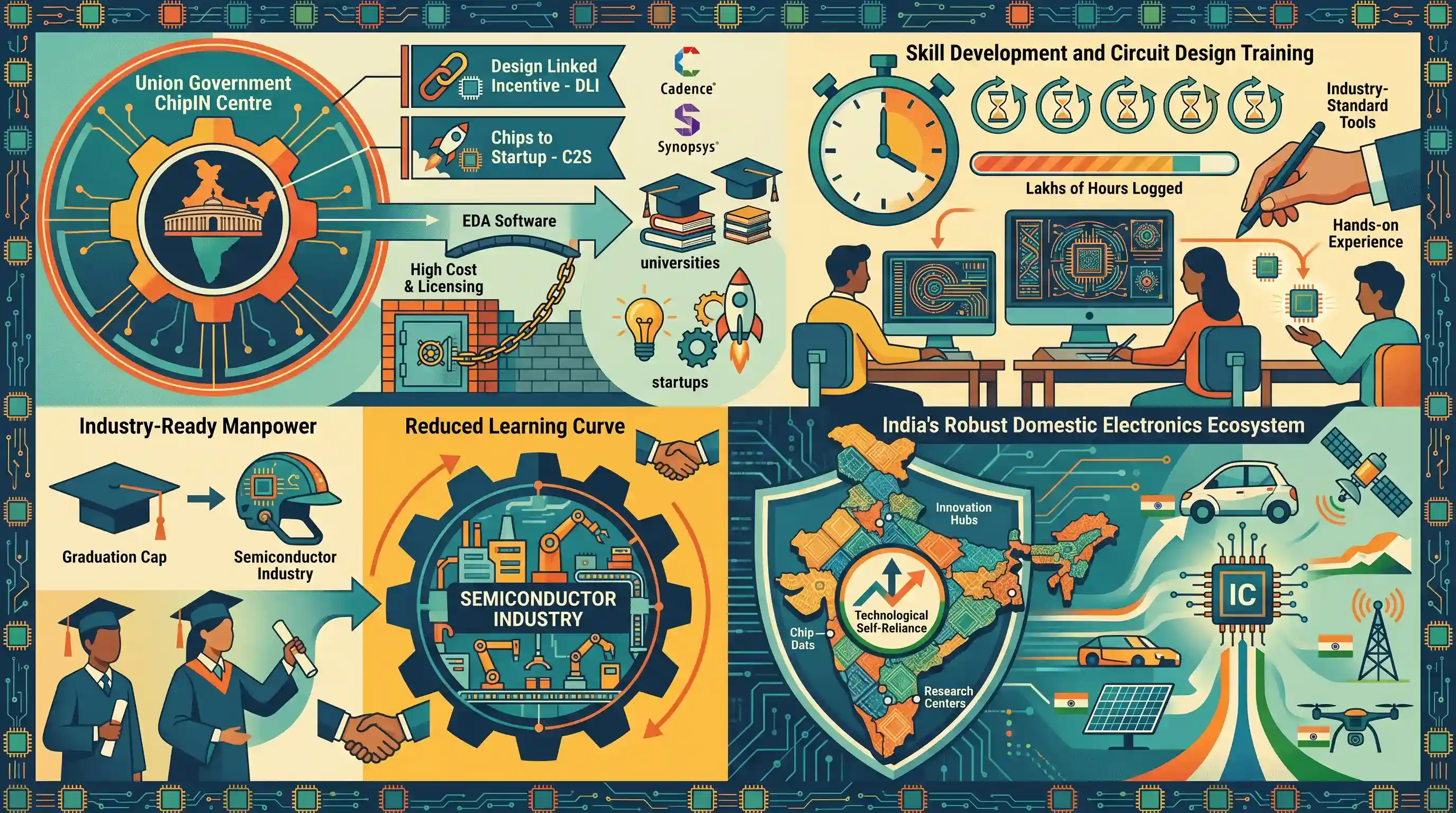
The Union Government's ChipIN Centre is driving skill development and technological self-reliance by licensing expensive Electronic Design Automation (EDA) software and offering free access to Indian universities and startups. Operating under the Design Linked Incentive and Chips to Startup schemes, the initiative gives students hands-on experience with industry-standard tools from vendors like Cadence and Synopsys. MeitY data reveals that students at top engineering institutes have logged lakhs of hours designing circuits, thereby democratizing access to chip design infrastructure. This hands-on training generates industry-ready manpower, reducing the learning curve for graduates entering the semiconductor industry and bolstering India's ambitions for a robust domestic electronics ecosystem.
Key Points
- The ChipIN Centre licenses costly Electronic Design Automation (EDA) software and provides it for free to startups and 240 universities.
- The initiative operates under the government's Design Linked Incentive (DLI) and Chips to Startup schemes.
- Students and researchers have logged lakhs of hours using tools from major industry vendors like Synopsys and Cadence.
- Access to these standardized tools creates industry-ready manpower by minimizing the learning curve for fresh graduates and interns.
- The democratization of chip design infrastructure is seen as a vital step towards establishing a self-reliant semiconductor ecosystem in India.
Important Terms
ChipIN Centre

A centralized facility at C-DAC Bengaluru providing students and startups with shared access to expensive Electronic Design Automation (EDA) tools, compute resources, and fabrication services for semiconductor design.
UPSC context
GS Paper 3: Science and Technology — Indigenization of Technology; significant as a hub for 'Atmanirbhar Bharat' in high-tech design.
Chips to Startup (C2S) Programme
A MeitY capacity-building initiative aiming to train 85,000 industry-ready professionals in VLSI and embedded systems design over five years through academic and industry collaboration.
UPSC context
GS Paper 2: Government Policies and Interventions; GS Paper 3: Skill development in the semiconductor value chain.
Design Linked Incentive (DLI) Scheme
A scheme providing financial incentives and infrastructure support to domestic companies and startups for semiconductor design, development, and deployment, aiming to foster an indigenous fabless ecosystem.
UPSC context
GS Paper 3: Indian Economy and Industrial Policy; tests understanding of fiscal support for strategic deep-tech sectors.
Electronic Design Automation (EDA) Tools
Specialized software tools used by engineers to design, simulate, verify, and manufacture complex integrated circuits (ICs) and printed circuit boards (PCBs).
UPSC context
GS Paper 3: IT and Computers; highlights the software-heavy nature of semiconductor design versus manufacturing.
India Semiconductor Mission (ISM)
The umbrella mission launched with a ₹76,000 crore outlay to build a sustainable semiconductor and display ecosystem in India through fabrication, design, and assembly incentives.
UPSC context
GS Paper 3: Science and Technology/Economy; critical for questions on technological self-reliance and global value chains.
Ministry of Electronics and Information Technology (MeitY)
The nodal Union Ministry responsible for policy formulation and implementation of IT, electronics, and digital governance initiatives, including the India Semiconductor Mission.
UPSC context
General context for any digital/electronics policy questions in Prelims or Mains.
Prelims Trap
The ChipIN Centre provides physical fabrication facilities to startups under the Production Linked Incentive (PLI) scheme.
ChipIN provides centralized access to software (EDA tools) for chip design, not physical fabrication hardware. It operates under the Design Linked Incentive (DLI), focusing on fabless design rather than manufacturing.
Static Concepts Connected
How does the Design Linked Incentive (DLI) Scheme function within India's semiconductor ecosystem?
- Fabless Focus: Unlike PLI which targets physical manufacturing (fabs), DLI supports fabless startups creating semiconductor designs and intellectual property.
- Financial Support: Provides up to 50% reimbursement on eligible design expenditure and 4-6% deployment-linked incentives on net sales of chip designs.
- Nodal Agency: Implemented by the Centre for Development of Advanced Computing (C-DAC), an autonomous scientific society under MeitY.
What role do Electronic Design Automation (EDA) tools play in the semiconductor industry?
- Software Core: EDA comprises complex software tools necessary for designing, simulating, and validating modern Integrated Circuits (ICs) and PCBs.
- High Cost Barrier: The software is highly expensive and globally dominated by a few firms, creating massive entry barriers for new startups.
- Strategic Access: By centralizing EDA licensing, India democratizes chip design access, accelerating domestic technological self-reliance and creating industry-ready talent.
Cross-Topic Patterns
Geopolitics + Demographic Dividend
While India currently lacks advanced physical fabs, skilling engineers via C2S leverages India's demographic dividend to capture the lucrative global 'fabless' design market amidst US-China supply chain decoupling.
Intellectual Property + Deep Tech startups
Shifting from traditional IT services to deep tech product creation requires robust IP generation. DLI directly incentivizes domestic IP ownership in integrated circuits, which is crucial for strategic autonomy.

Expect a 2026 Prelims question testing the subtle differences between PLI, DLI, and SPECS under the umbrella India Semiconductor Mission.
Linked PYQs · 3
Linked PYQs · 3
- 2025MainsGS3
India aims to become a semiconductor manufacturing hub. What are the challenges faced by the semiconductor industry in India? Mention the salient features of the India Semiconductor Mission.
- 2023MainsGS2
Skill development programmes have succeeded in increasing human resources supply to various sectors. In the context of the statement analyse the linkages between education, skill and employment.
- 2025MainsGS3
Discuss the rationale of the Production Linked Incentive (PLI) scheme. What are its achievements? In what way can the functioning and outcomes of the scheme be improved?
