Cabinet Approves HCL Foxconn Semiconductor Plant
Source:Indian Express ↗
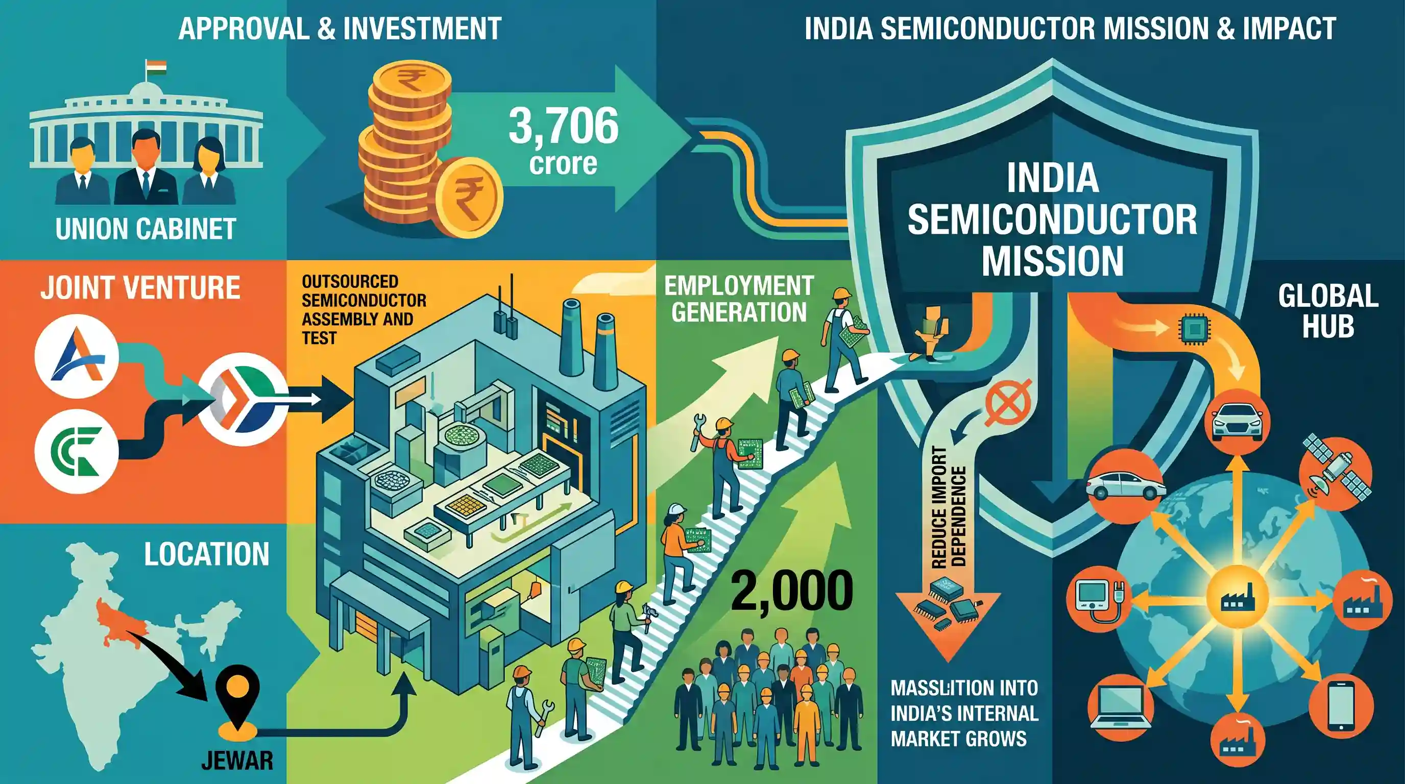
Why It Matters
Illustrates the tangible progress of the India Semiconductor Mission and highlights the role of foreign joint ventures (FDI) in acquiring critical technological capabilities and generating regional employment.
Summary
The Union Cabinet has approved a Rs 3,706 crore joint venture between HCL and Foxconn to establish an Outsourced Semiconductor Assembly and Test (OSAT) facility in Jewar, Uttar Pradesh. The project is anticipated to generate 2,000 jobs and marks a critical milestone for the India Semiconductor Mission, which seeks to reduce import dependence and position India as a global hub for electronics manufacturing.
Key Points
- The Union Cabinet has approved a semiconductor joint venture (JV) between IT major HCL and Taiwan's Foxconn.
- The joint venture will be located in Jewar, Uttar Pradesh.
- The project entails an investment of Rs 3,706 crore.
- It is expected to create 2,000 direct and indirect jobs in the region.
- The facility represents a significant step under the India Semiconductor Mission to build a robust domestic electronics manufacturing ecosystem.
Important Terms
India Semiconductor Mission (ISM)

A nodal agency-led initiative with a ₹76,000 crore outlay to develop a sustainable semiconductor and display ecosystem, aiming to position India as a global electronics manufacturing hub.
UPSC context
GS Paper 3: Industrial Policy and S&T. Tests knowledge of self-reliance (Atmanirbhar Bharat) and critical technology infrastructure.
Outsourced Semiconductor Assembly and Test (OSAT)
A third-party service model in the semiconductor value chain focused on the post-fabrication stages of assembling, packaging, and testing integrated circuits before they are integrated into devices.
UPSC context
GS Paper 3: Science and Technology. Relevant for understanding the global supply chain and India's strategic entry into electronics manufacturing.
HCL-Foxconn Joint Venture
A 60:40 partnership between India’s HCL Group and Taiwan’s Foxconn to establish UP's first OSAT facility, specifically targeting the production of display driver chips for electronics and automobiles.
UPSC context
GS Paper 3: Investment Models. Tests understanding of Foreign Direct Investment (FDI) and technology transfer through international industrial collaborations.
Production Linked Incentive (PLI) Scheme
A government mechanism providing fiscal support (up to 50% for fabs and 30% for OSAT) to domestic and international companies to boost local manufacturing and reduce import dependency.
UPSC context
GS Paper 3: Indian Economy. Key tool for industrial growth, exports, and 'Make in India' objectives.
Display Driver Chips
Specialized integrated circuits that act as an interface between a microprocessor and a display (LCD/OLED), controlling the image rendering on smartphones, laptops, and automotive screens.
UPSC context
GS Paper 3: Science and Technology. Tests awareness of specific components within the indigenization of technology and electronics.
MeitY (Ministry of Electronics and Information Technology)
The nodal ministry responsible for formulating and implementing policies related to electronics, IT, and the India Semiconductor Mission to drive digital transformation and technological sovereignty.
UPSC context
GS Paper 2: Government Policies. Tests knowledge of institutional frameworks governing the digital and high-tech sectors.
Prelims Trap
"The newly approved HCL-Foxconn facility in Uttar Pradesh will manufacture silicon wafers and fabricate semiconductor chips locally."
The facility is an OSAT unit. It only packages and tests chips fabricated elsewhere; it does not manufacture the raw silicon wafers (Fab) itself.
Static Concepts Connected
What are the core stages of the semiconductor manufacturing value chain?
- Design: Creating the integrated circuit blueprints and architecture. India already has a strong global market share in this talent-heavy segment.
- Fabrication (Fab): Manufacturing the actual integrated circuits on silicon wafers. This is extremely capital-intensive and the hardest stage to indigenize.
- OSAT / ATMP: Outsourced Semiconductor Assembly and Test (OSAT) involves packaging the fabricated chips and testing them before deployment into consumer devices.
What are the key features of the India Semiconductor Mission (ISM)?
- Nodal Agency: It operates as an independent business division within the Digital India Corporation under the Ministry of Electronics and IT (MeitY).
- Financial Incentives: Provides a flat 50% capital subsidy on a pari-passu (equal footing) basis for setting up Fabs, OSATs, and compound semiconductor units.
- Ecosystem Approach: Focuses simultaneously on chip design (Design Linked Incentive), wafer fabrication, and packaging to avoid supply chain bottlenecks.
Cross-Topic Patterns
Geopolitics + Supply Chain Resilience
Shifting OSAT facilities to India aligns with the Quad Semiconductor Supply Chain Initiative and the 'China Plus One' strategy to de-risk global electronics manufacturing dependencies.
Geography: High-Tech Location Factors
Selecting Jewar (UP) over traditional southern IT hubs highlights how greenfield infrastructure (new airports), land banks, and state-level subsidies are shifting industrial agglomeration for electronics.

Expect a 2026 Prelims question testing the technical difference between OSAT and Fab, paired with ISM's 50% funding mechanism.
Linked PYQs · 2
Linked PYQs · 2
- 2025MainsGS3
India aims to become a semiconductor manufacturing hub. What are the challenges faced by the semiconductor industry in India? Mention the salient features of the India Semiconductor Mission.
- 2016MainsGS3
Justify the need for FDI for the development of the Indian economy. Why there is gap between MOUs signed and actual FDIs? Suggest remedial steps to be taken for increasing actual FDIs in India.
