New Vande Bharat Corridors and Semiconductor Milestones
Source:Indian Express ↗
Why It Matters
The article covers vital GS3 themes: infrastructure development through high-speed rail networks, and India's growing capabilities in the semiconductor sector. Both areas are crucial for India's aspirations of rapid economic growth and becoming a global manufacturing hub.
Summary
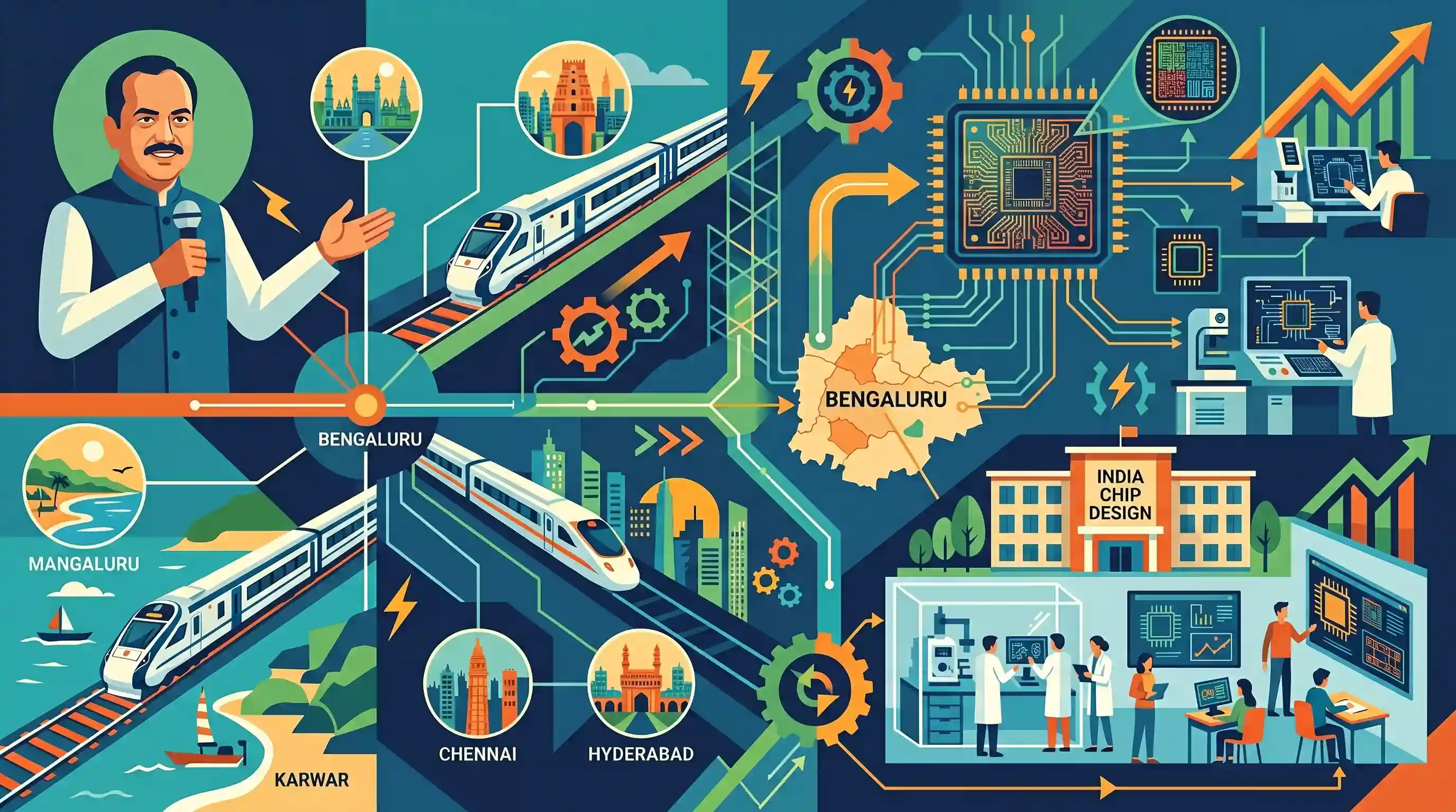
Union Minister Ashwini Vaishnaw announced new Vande Bharat Express routes connecting Bengaluru to Mangaluru and Karwar, and highlighted the approval of high-speed rail corridors from Bengaluru to Chennai and Hyderabad. In the technology sector, a 2 nm semiconductor chip designed by Qualcomm was launched in Bengaluru, underlining India's growing semiconductor capabilities and the integration of advanced chip design tools into university curricula.
Key Points
- A new Vande Bharat route is announced to connect Bengaluru with Mangaluru and Karwar, alongside ongoing track electrification between Hassan and Mangaluru.
- Karnataka received a record railway budget allocation of Rs 7,748 crore.
- High-speed rail links from Bengaluru to Chennai (expected 73-minute travel time) and to Hyderabad (approximately 2 hours) have been approved.
- Qualcomm launched a 2 nm semiconductor chip designed in Bengaluru, marking a milestone in India's semiconductor ecosystem.
- Over 300 Indian universities have integrated Electronic Design Automation (EDA) tools from Synopsis, Cadence, and Siemens to train students in chip design.
Important Terms
India Semiconductor Mission (ISM)

A comprehensive policy initiative aimed at building a self-reliant semiconductor and display manufacturing ecosystem, reducing import dependency and securing global supply chain integration.
UPSC context
GS Paper 3: Science & Technology; Indigenization of technology; Strategic industrial policy for electronics manufacturing.
Vande Bharat Express
India's first semi-high-speed, indigenously designed, and self-propelled trainset; features advanced safety systems like Kavach and modern passenger amenities for inter-city travel.
UPSC context
GS Paper 3: Infrastructure; Modernization of Indian Railways; 'Make in India' in the transport sector.
Electronic Design Automation (EDA) Tools
Category of software tools used to design, verify, and manufacture complex integrated circuits (ICs) and electronic systems, critical for modern semiconductor engineering.
UPSC context
GS Paper 3: Science & Technology; High-end semiconductor design capabilities; Skill development in deep tech.
Indian Railways
The departmental body under the Ministry of Railways that operates India's rail network, currently undergoing massive modernization through high-speed corridors and station redevelopment.
UPSC context
GS Paper 3: Infrastructure (Railways); Economic development through connectivity; Public sector asset management.
Qualcomm
A leading American multinational semiconductor company that designs and markets wireless telecommunications products and chips, significantly expanding its R&D footprint in India.
UPSC context
GS Paper 3: Role of private players in technology indigenization and the global value chain.
Chips to Startups (C2S) Initiative
A MeitY initiative to train 85,000 professionals in chip design by providing academic institutions access to industry-standard EDA tools and fabrication support.
UPSC context
GS Paper 3: Human capital development; Industry-academia collaboration; Startup ecosystem in electronics.
Prelims Trap
India recently successfully manufactured a cutting-edge 2nm semiconductor chip locally.
India's engineers DESIGNED the 2nm chip, but fabrication occurs abroad. Current domestic manufacturing capabilities target mature nodes (28nm+), not cutting-edge 2nm physical manufacturing.
Static Concepts Connected
What does a nanometer (nm) node signify in semiconductor chips?
- Generational marker: Originally denoted physical gate length, but now serves as a marketing term for a new generation of chip architecture.
- Transistor density: Smaller nodes allow billions more transistors on a single chip, vastly increasing processing power and AI workload capabilities.
- Energy efficiency: Reduces the distance electrons travel, significantly lowering power consumption and heat generation.
Difference between High-Speed Rail (HSR) and Semi-High Speed Rail?
- High-Speed Rail: Operates on dedicated standard-gauge tracks at speeds exceeding 250 km/h (e.g., proposed bullet trains for Chennai/Hyderabad corridors).
- Semi-High Speed: Operates on upgraded existing broad-gauge tracks at speeds of 160-200 km/h (e.g., Vande Bharat Express).
Cross-Topic Patterns
Chip Design and Skilling Initiatives
The integration of EDA tools in universities highlights the MeitY 'Chips to Startup' (C2S) scheme, linking deep-tech industrial policy with the New Education Policy's focus on technical employability.
Ghats railway tracks and ecological sensitivity
Expanding track electrification and train frequency in the Hassan-Mangaluru section frequently sparks UPSC mains questions on balancing transit infrastructure with the ecological fragility of the Western Ghats.

Expect a multi-statement Prelims question contrasting India's chip design dominance with its nascent semiconductor fabrication stage.
Linked PYQs · 3
Linked PYQs · 3
- 2022MainsGS3
Why is Public Private Partnership (PPP) required in infrastructural projects ? Examine the role of PPP model in the redevelopment of Railway Stations in India.
- 2021MainsGS3
“Investment in infrastructure is essential for more rapid and inclusive economic growth.” Discuss in the light of India's experience.
- 2025MainsGS3
India aims to become a semiconductor manufacturing hub. What are the challenges faced by the semiconductor industry in India? Mention the salient features of the India Semiconductor Mission.
