Semiconductor OSAT Facility Groundbreaking Held in Visakhapatnam
Source:evertiq ↗
ఇది ఎందుకు ముఖ్యం
The creation of a robust domestic semiconductor packaging (OSAT) ecosystem is vital for India's strategic autonomy in electronics and technology. This massive investment in Visakhapatnam marks a crucial step in transforming Andhra Pradesh into a high-tech manufacturing hub and aligns with national self-reliance goals.
సారాంశం
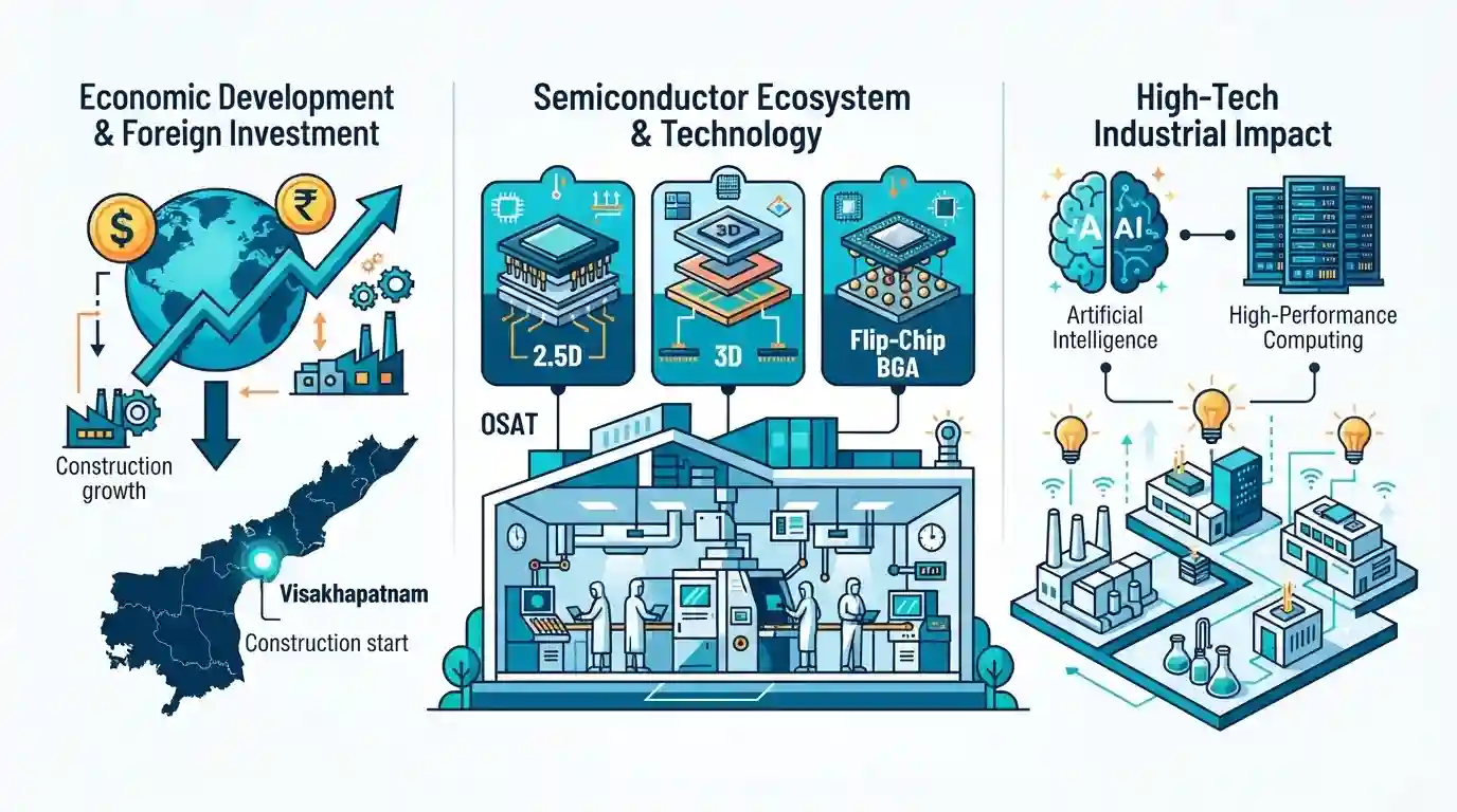
ASIP Technologies, an electronics manufacturing firm based in Hyderabad, has initiated construction on a $260 million Outsourced Semiconductor Assembly and Test (OSAT) facility in Visakhapatnam, Andhra Pradesh. Supported by the state government and foreign investment, the plant will deliver advanced semiconductor packaging solutions, including 2.5D, 3D, and Flip-Chip BGA technologies. The facility is expected to cater to high-demand sectors such as artificial intelligence and high-performance computing, thereby strengthening India's domestic semiconductor ecosystem and fostering high-tech industrial development in Andhra Pradesh.
ముఖ్య అంశాలు
- Hyderabad-based ASIP Technologies has broken ground on a $260 million Outsourced Semiconductor Assembly and Test (OSAT) facility in Visakhapatnam.
- The project is backed by foreign investors and the Andhra Pradesh state government.
- The facility will focus on advanced semiconductor packaging technologies such as 2.5D, 3D, and Flip-Chip BGA.
- This development aims to supply components for AI, high-performance computing, and other advanced tech sectors, bolstering local and national electronics manufacturing.
ముఖ్యమైన పదాలు
ASIP Technologies

A Hyderabad-based electronics firm establishing a $260 million semiconductor packaging plant in Visakhapatnam. It represents South India's first OSAT project approved under the India Semiconductor Mission.
UPSC context
GS-3 (Industrial Growth). Demonstrates private sector integration into India's emerging high-tech domestic manufacturing ecosystem.
Outsourced Semiconductor Assembly and Test (OSAT)
Third-party manufacturing facilities that assemble, package, and test semiconductor chips. They process raw fabricated silicon dies into finished microchips ready for integration into electronic devices.
UPSC context
GS-3 (Science & Tech, Indigenization). Essential for India to reduce import dependence and complete its domestic semiconductor value chain.
Andhra Pradesh Semiconductor & Display Fab Policy 2024-29
A state industrial policy offering up to a 30% capital subsidy on top of central grants to attract mega investments in semiconductor fabrication, OSAT, and display manufacturing.
UPSC context
GS-3 (Investment Models). Highlights competitive federalism and state-level financial incentives crucial for realizing India's high-tech electronics manufacturing ambitions.
Flip-Chip BGA (Ball Grid Array)
An advanced semiconductor packaging technology where the silicon die is flipped face-down and connected directly to the substrate via solder bumps, enabling higher speeds and signal density.
UPSC context
GS-3 (IT & Computers). Represents the advanced technological capabilities India is domesticating to support high-performance computing and AI hardware.
India Semiconductor Mission (ISM)
A dedicated nodal initiative under MEITY offering substantial fiscal incentives to build a vibrant domestic semiconductor and display manufacturing ecosystem in India.
UPSC context
GS-3 (Government Policies). The primary state-backed driver behind India’s push for strategic autonomy in electronics and global chip supply chains.
ప్రిలిమ్స్ ఉచ్చు
The new Visakhapatnam facility will manufacture silicon wafers to boost India's self-reliance in the semiconductor sector.
OSAT facilities do NOT manufacture silicon wafers. They only package and test chips fabricated elsewhere. Conflating Fab (manufacturing) with OSAT (assembly) is a classic trap.
అనుసంధానమైన స్థిర భావనలు
What is the difference between a Semiconductor Fab and an OSAT facility?
- Fab (Fabrication): Manufactures the actual integrated circuits (ICs) on raw silicon wafers using highly capital-intensive processes like photolithography.
- OSAT / ATMP: Stands for Outsourced Semiconductor Assembly and Test. It takes manufactured silicon wafers, dices them, protects them in packages, and tests them.
- Advanced Packaging: Involves stacking multiple chips (like 2.5D or 3D) within a single package to increase processing speeds for AI and computing without shrinking chip nodes.
What are the core fiscal incentives under the India Semiconductor Mission (ISM)?
- Nodal Agency: Established under the Digital India Corporation (MeitY) as the nodal agency to build a robust domestic semiconductor and display ecosystem.
- Fab Subsidies: Provides up to 50% of the project cost on a pari-passu basis for setting up Semiconductor Fabs across all technology nodes.
- OSAT / ATMP Support: Offers 50% capital expenditure support for setting up approved ATMP and OSAT facilities in India, crucial for building the downstream supply chain.
అంతర-అంశ నమూనాలు
Semiconductors & Coastal Industrial Corridors
High-tech OSAT clusters are mapping onto nodes of the Visakhapatnam-Chennai Industrial Corridor (VCIC), leveraging deep-water ports for the seamless import of raw silicon and export of packaged components.
AI Bottlenecks & Advanced Packaging Geopolitics
As Moore's Law slows, 2.5D/3D advanced packaging has become the new geopolitical choke point for AI. Nations are realizing OSATs are as critical as Fabs for high-performance computing.

Expect a 2026 prelims question testing the technical difference between Silicon Fabs and OSAT/ATMP within the India Semiconductor Mission.
అనుసంధాన PYQలు · 2
అనుసంధాన PYQలు · 2
- 2024APPSC_PRELIMSGS1
Which of the following statement/statements is/are incorrect regarding the Andhra Pradesh Industrial Policy 2023 - 27? I. To achieve a minimum contribution of 25% by industry in the State GDP II. To provide end-to-end facilitation in 2 weeks III. To envisage ten (10) priorities of accomplishment IV. To focus on becoming a 'Plug and Play State' for investments V. Ensuring land allotment by APIIC within a period of 2 weeks upon receipt of application Select the answer using the codes given below :
- 2008APPSC_PRELIMSGS1
Which of the following is a natural harbour in Andhra Pradesh?
